اطلاعیه

Collapse
No announcement yet.

Auto Placer

Collapse
X
 
  • فیلتر
  • زمان
  • Show
Clear All
new posts

    Auto Placer

    با سلام
    من شنیدم آلتیوم قابلیت Auto Placer داره که خودش چیدمان میکنه قطعاتو ولی خودم تا حالا ندیدم
    گفتم این تاپیکو ایجاد کنم شاید کسی دیده باشه یا باش کار کرده باشه ما هم یاد بگیریم
    اگر کسی با Auto Placer کار کرده ممنون میشم آموزششو اینجا بذاره
    درایور شبکه و nRF24L01
    کاتالوگ محصولات
    کنترلر CNC شش محوره براي پرينتر 3D و Pick n Place
    شبيه ساز تک تيرانداز و سيبل ديجيتال با پردازش تصوير
    فروش اسيلوسکوپ GWinstek GOS-630FC

    #2
    پاسخ : Auto Placer

    من که کلا از جواب گرفتن نا امیدم :sad:
    آبی اینجا برا ما گرم نمیشه
    خب خودم شروع میکنم به یه چیزایی گفتن ببینم میشه با هم تکمیلش کنیم چون واقعا خودم وقتم پره و نمیتونم بش ور برم تا زیرو خمشو در بیارم
    درایور شبکه و nRF24L01
    کاتالوگ محصولات
    کنترلر CNC شش محوره براي پرينتر 3D و Pick n Place
    شبيه ساز تک تيرانداز و سيبل ديجيتال با پردازش تصوير
    فروش اسيلوسکوپ GWinstek GOS-630FC

    دیدگاه


      #3
      پاسخ : Auto Placer

      Protel DXP system has two built-in software components avtorazmescheniya - Cluster Placer and Statistical Placer. The first fully integrated in the PCB editor, well-managed and is recommended for use with the boards with the number of components is not more than 100. The second program is running as an additional module and uses a fundamentally different algorithm, which analyzes the length of the chains and with a large number of components. But in general, both programs provide poor result and can be recommended only as an auxiliary tool for the interactive placement, when some components previously placed manually and locked. Consider the work of these programs.

      Make a copy of the printed circuit board developed by us for future experiments, which will open in the editor PCB document Multivibrator. PcbDoc and execute the menu command File / Save Copy As and name the file Multivibrator1.PcbDoc.
      With the command File / Open Multivibrator1.PcbDoc open file as a free document.

      Remove all existing wires on the board so they do not interfere with us.

      Right-click any empty space of the PCB on the shortcut menu, click Build Query (hot keys SHIFT + B). A dialog box Building Query From Board (Figure 1).


      Here in the column Condition Type / Operator drop-down list Add First Condition will select Belongs to Net Class, which means that the selection of all objects belonging to this class of circuits.

      Our board has only one is the default class of chains All Nets, who will appear in the column Condition Value. On the right column Query Preview displays a text description of the query InNetClass («All Nets»).

      Check whether the flag Select Matching.
      Click OK or press Enter.

      The editor printed circuit boards will be allocated all of the conductors.

      Remove all guides by pressing Delete.
      Save the changes to the document by pressing the hot keys F, S.

      Avtorazmeschenie using Cluster Placer

      We define the design rules that define the minimum clearances between the components on the board and recorded the program Cluster Placer in the process.

      Menu command Design / Rules (hotkey D, R). Open the already familiar dialog PCB Rules and Constraints Editor, which set the rules of design.

      Note that when you create a category Placement blank cards were automatically given two rules Height and Component Clearance. The first rule governs the height of the component, and for us now is not very important, and the second is the distance between the components on the board.

      Perform left-click on the rule Component Clearance. The right pane will open a description of the rule (2).


      Type in the new name for the rule Name: "General."

      Also record the scope of the rule. The scope of a subset of objects on a printed circuit board, which is covered by this rule. By way of reference of the rule are divided into unary and binary. An example of a unary rules can be considered earlier limitation on the width of the conductor. In the description of binary rules specify two subsets of objects, so in this case (Fig. 2) the scope is described as' between all the components and all the components. " At first glance, such a system seems overly complicated, but it allows you to specify the editor printed circuit boards well-understood criteria for verification of the design process. We will not change these settings.

      At the bottom, in the Gap define a new value of the gap 2 mm.

      Then in the drop down list should indicate Check Mode Test mode rules. Mode Quick Check (quick scan) does not permit the imposition of the components, in whatever bed they may be, and as a boundary component uses a rectangle around all the component primitives (without text). Multi Layer Check Mode also limits component rectangle, but takes into account the layer on which the component is located and allow the case shown in Figure 3. The third mode Full Check checks the overlay components to each other with all their component graphics primitives. However, it only works in the batch design rule checking (DRC).


      Since all components on our board will be located on only one (upper) side, then switch to Quick Check.

      Create a new rule governing the distance between transistors.

      Right-click on the type of rules Component Clearance on the shortcut menu, click New Rule.
      Left-click on the newly created rule. In the right pane to open a description.
      In the Name window, give a name rule "between the transistors."
      Further in the field Where the First object matches (the first subset of objects), select Advanced (Query) and click the Query Builder. A window Building Query From Board (Figure 4).


      Here in the column Condition Type / Operator drop-down list Add First Condition will select Belongs to Component (a component).
      In the Condition Value column displays a list of all the components from which to choose the transistor VT1. On the right column Query Preview displays a text description of the query InComponent ('VT1&#039
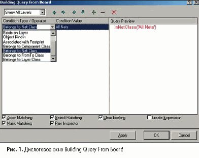
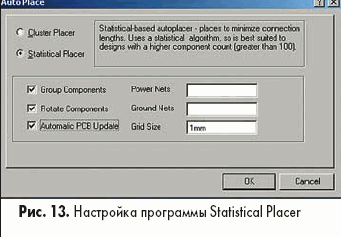
. To save the results, click OK.
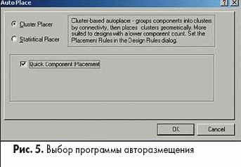
      Further in the field Where the Second object matches (second subset of objects) also will select the Advanced (Query), press the button Query Builder and then in the wizard queries indicate transistor VT2. On the right column Query Preview displays a text description of the query InComponent ('VT2&#039. Click OK.
      At the bottom of the Rule Description box Gap define a new value gap 5 mm.
      In the drop-down list, select Profiles Check Mode Quick Check.

      I created the rule prescribes to place transistors no closer than 5 mm to each other. Create another rule of this type, which regulates the gaps between the transistors and all other components.

      Right-click on the type of rules Component Clearance on the shortcut menu, click New Rule.
      Left-click on the newly created rule. In the right pane to open a description.
      In the Name window, give a name rule "between the transistors and all the rest."
      Further in the field Where the First object matches (the first subset of objects), select Advanced (Query) and click the Query Helper. Will be familiar to us on the previous lesson window Query Helper.
      Clear the Query, then click in to the left mouse button, select all of its contents by pressing the key combination Ctrl + A and then press Delete.
      In the bottom left will click on a category of actions Membership Check (membership test). In the box on the right displays a list of available functions, checking membership.
      Double-click the left mouse button on the operator InComponent. In the Query Designer will feature InComponent drop-down list, select the component offering. We select transistor VT1.
      Press the button Or (OR).
      Click again on the category of actions Membership Check.
      Double-click the left mouse button on the operator InComponent. In the query designer after the operator Or will function InComponent drop-down list, select the component offering. We select transistor VT2.
      Press the button Check Syntax, to check the accuracy of the request.
      Close the Query Builder by clicking on the button OK. Thus, the first subset of the request will be described InComponent (VT1) Or InComponent (VT2). Second subset left unchanged - All (all components).
      At the bottom of the Rule Description box Gap define a new value of the gap - 3mm.
      In the drop-down list, select Profiles Check Mode Quick Check.

      I created the rule prescribes to place transistors VT1 or VT2 at a distance no closer than 3 mm from any other components. Note that if we had ten or a hundred transistors to build a query would be tedious, so in Protel DXP system uses the concept of classes of objects, allowing to group them according to certain criteria (eg, classes, components or applications), thus significantly simplifying the management of the designing. Later we will consider a class of objects in more detail.

      Clicking on the Close button will close the dialog box PCB Rules and Constraints Editor.
      Save the changes to the document by pressing the hot keys F, S.

      Now we are fully prepared to fulfill avtorazmescheniya components. Here the reader might wonder why we did it, and if the board is so very simple? The answer is obvious: we did it, to understand the basic principles of management tools avtorazmescheniya that in the future will help us to handle more complex boards.

      Traditionally, automatic placement with most programs is bad. However, in some cases, to blame the users themselves who are neglected by the preparatory phase. The worse (or did) you describe the criteria that the program should use placement in, the worse (or no) will be obtained.


      Menu command Tools / Auto Placement / Auto Placer ...
      In the next window select the option Auto Place Cluster Placer and switch Quick Component Placement enable rapid deployment mode.
      Pressing OK will launch the process of accommodation.

      The program will perform the "fast" component placement, starting with the lower left corner with the circuit board on the layer Keep-Out. Note that some components are highlighted in green, which indicates the presence of design rule violations.

      Go to the control panel editor of printed circuit boards and in the drop down list, select the type of scanned objects Rules.
      At the bottom of the pane displays a list of violations, two of which relate to the rules of type Component Clearance, and the other with a small gap between the pads and lines on the layer Keep-Out. Left-click on any of the violations in the list to view its essence. When you are finished violations Left-click anywhere on the board, pressing Shift + C masking cast off objects and return the optimal zoom in by pressing the hot keys V, F.

      Perform close-repulsion components with a special tool Shove, but before that set it up.


      Menu command Tools / Auto Placement / Set Shove Depth.
      In the window Shove Depth define depth repulsion 5. Under this concept here means the maximum number of repulsive components in compliance with the rules of control gaps. This number can range from 1 to 1000, but in practice for relatively simple boards should ask him no more than 5 -10, to make it easy to keep track of your changes. Close the window.
      Menu command Tools / Auto Placement / Shove.
      Move the mouse, taking the form of the cross, one of the items highlighted in green indicate disorders such as resistor R3, and perform one-click.

      All components located around the resistor R3, will be moved in different directions so that the control rule gap between them (Fig. 7).


      Exit repulsion, which press ESC or right-click anywhere in the drawing.
      Save the changes to the document by pressing the hot keys F, S.

      Consider another program mode avtorazmescheniya Cluster Placer.

      Menu command Tools / Auto Placement / Auto Placer ...
      In the next window select the option Auto Place Cluster Placer and switch Quick Component Placement disable rapid deployment.
      Pressing OK will launch the process of accommodation.

      The program will perform a "slow" component placement, which analyzes the list of compounds for optimization of the bond lengths, and also takes into account an increasing number of design rules (Figure 8). Please note that in this case the extreme components are separated from the circuit on the Keep-Out layer, such that they cause the previously observed violations of the gaps between the pads and the circuit Keep-Out.


      Note that in this mode, the program runs more slowly than the more components on the board, and with more than 100 of them may complete system crash Protel DXP, due to a lack of memory. The progress of the placement can be tracked on line in the status bar at the bottom left of the screen.

      Great influence on the speed component placement has difficulty bonding between them, so it is advisable to exclude from the analysis of the longest chain, what, as a rule, the power supply and ground. This is done by using a special type of design rules Nets to Ignore Placement category and is recommended for multi-layer boards with internal power and ground layers. Our duplex board power supply and grounding are essential and determine the entire topology, and avoiding them is not desirable.

      In addition to the above design rules Component Clearance and Nets to Ignore Cluster Placer program keeps track of the four types of rules: Component Orientations (the orientation of the components), Permitted Layers (layers allowed), Height (height components) and Room Definition (field placement). The first three rules is obvious, and their definition can be performed independently as a workout, but the final rule, Room Definition, requires special consideration.

      Avtorazmeschenie with areas Room Definition

      To understand how the siting Room Definition, perform the following exercise.

      Clean up the blank cards, for which the coverage window select all the components on the board and hold the left mouse button and drag them to the right beyond the board.
      Menu command Design / Rooms / Place Rectangular Rooms. The mouse pointer changes to a crosshair with a red square in the center.
      Tab key will call window for editing rules Room Definition (Figure 9).

      درایور شبکه و nRF24L01
      کاتالوگ محصولات
      کنترلر CNC شش محوره براي پرينتر 3D و Pick n Place
      شبيه ساز تک تيرانداز و سيبل ديجيتال با پردازش تصوير
      فروش اسيلوسکوپ GWinstek GOS-630FC

      دیدگاه


        #4
        پاسخ : Auto Placer


        In the Name field, specify the name of: "Transistors".
        Further in the field Where the First object matches (the first subset of objects), select Advanced (Query).
        Entered in the Full Query already familiar query text selection transistors InComponent (VT1) Or InComponent (VT2) or use it to build the Query Query Helper.
        The drop-down list at the bottom of the Edit Room Definition, define a condition of processing components Keep Object Inside (objects must be inside).
        In the combo box just above the layer define placement TopLayer.
        Save your settings and close the window by clicking OK. The system will return to the drawing.
        Clicked the left mouse button near the top left corner of the board, what we define the first corner of the rectangle.
        Move the mouse to the right down about a third of the board and once again click the left mouse button.

        You will see a shaded rectangle, highlighted in green, indicating that the presence of disturbances. It is easy to guess that the violation is that the transistors are out of a certain area of ​​accommodation for them. Guess you can check on the tab panel PCB editor printed circuit boards.

        We set the second area.

        Press Tab, than call the rule editing window Room Definition.
        In the Name field, specify the name of "VseOstalnye" (no space required!).
        Leave the area of ​​the rule as All (all). Later we will change it.
        The drop-down list at the bottom of the Edit Room Definition, define a condition of processing components Keep Object Inside (objects must be inside).
        In the combo box just above the layer define placement TopLayer.
        Save your settings and close the window by clicking OK. The system will return to the drawing.
        Perform a left click just below the first area than define the first corner of the rectangle.
        Move the mouse to the bottom right corner of the board, and again click the left mouse button.

        The second area of ​​placement takes the remaining two-thirds of the board (Figure 10).


        Describe the scope of the second rule "everything but transistors" we could and with a complex query, however, is more correct to create the corresponding component class.

        Menu command Design / Classes. A dialog box Object Class Explorer, which lists all the possible object classes. It is easy to see that the classes can be grouped chain (Net Classes), components (Component Classes), layers (Layer Classes), pads (Pad Classes), routes (From-To Classes) and channels (Design Channel Classes).
        Right-click on the class category Component Classes on the shortcut menu, click Add Class (add the class.) The list will be a new component class New Class.
        Let's click on it with the left mouse button. On the right, there will be two lists of objects. The first column of Non-Members will be listed components that are not included in this class. Members of the second column is empty.
        Successive clicks the left mouse button while holding down the Ctrl select in the first column of all components except the transistors VT1 and VT2.
        Click the icon> at the columns. The selected components are transferred to the second column.
        Finally, rename the newly created class, which press F2 and enter a new name: "Not transistors" (11).


        Close the Object Class Explorer window by pressing Close.
        We return to the definition of the second placing of "everything else", by performing on her double-click.
        Further in the field Where the First object matches (the first subset of objects), select Advanced (Query) and click the Query Builder. A window Building Query From Board.
        Here in the column Condition Type / Operator drop-down list Add First Condition will select Belongs to Component Class (included in class components).
        Condition Value column, a list of all the classes described in the project components (in this case two), from which you should select the class, "Do not transistors." To save the results, click OK. Request takes the form (InComponentClass ('Not transistors&#039).
        Save your settings and close the window by clicking OK.
        Save the changes to the document by pressing the hot keys F, S.

        Now you are ready for implementation avtorazmescheniya.

        Menu command Tools / Auto Placement / Auto Placer ...
        In the next window select the option Auto Place Cluster Placer and switch Quick Component Placement disable rapid deployment.
        Pressing OK will launch the process of accommodation.

        The output Cluster Placer will differ significantly from those obtained previously (12). Transistors will be available exclusively within their field placement, all other components - in the second field. Thus, the area of ​​Room Definition represent meaningful program management tool placement Cluster Placer. Considering that these areas and component classes can be created automatically when you transfer data from concept to design printed circuit boards, it is much easier for developers. More detail we consider this question in the study of tools for multi-channel design.


        Note also that in general the output of the program avtorazmescheniya Cluster Placer may be far from perfect, so it is recommended to run it several times in, keeping in between.

        Avtorazmeschenie using Statistical Placer

        The second program is designed for automatic placement processing boards with a large number of components (more than 100). It works on a fundamentally different algorithms and do not consider any of the above design rules. The main criterion for the correct placement of the components are considered to be a uniform distribution of components on the board at the optimum density of connections.

        Statistical Placer program does not interact with the areas Room Definition, so they can be removed.

        Hold down Shift, sequentially click on each of the areas of the left mouse button, and then press Delete.
        Menu command Tools / Auto Placement / Auto Placer ...
        In the next window select the option Auto Place Statistical Placer. At the bottom of the window will be located internal setting of the program.
        Enable the option Group Components (group components).
        Including the option to Rotate Components (rotated components).
        Be sure to include the option Automatic PCB Update (automatically update cost), so as not to lose the program received placement results.


        To facilitate the analysis of the bond lengths in the multi-layer boards with internal power and ground layers of the names of these circuits can be specified in the text boxes Power Nets and Ground Nets. For our board do not need.

        Pressing OK will launch the process of accommodation.

        Unlike programs Cluster Placer, which is fully integrated into the PCB editor of Protel DXP, Statistical Placer program has its own window, which displays the progress of the avtorazmescheniya. For our simple board avtorazmeschenie will do almost immediately, but for complex boards it may take tens of minutes. Percent complete optimization is displayed in the status bar. The density of the components shown colored squares of different sizes. For example, the view of one of the supplied example boards during avtorazmescheniya shown in Figure 14.


        Click OK in the message window on the completion of the placement. The system returns to the editor printed circuit boards, where the position of the components on the card will be automatically updated.
        To update the links, select all objects board (Ctrl + A), left-click on any of them, and deselect-clicking on a blank spot board.

        Locking components

        At the end of this tutorial will look at how the blocked components on the board.

        Double-click the left mouse button on any of the components. This opens a window for editing the parameters of the component.
        Including the option to Locked in the Component Properties.
        Close the window by clicking OK.

        Now the component is blocked from moving with the mouse, and you try to move it in the complex separation of components (for example, window coverage) will be issued a warning.

        Simultaneous locking (unlocking) of several components is done a little differently.

        Coverage window or by clicking the left mouse button while holding down Shift, select a group of components.
        Call the Inspector panel by clicking on the Inspect button at the bottom of the screen.
        Turn on (off) the option in line Locked panel Inspector.
        Press Enter.

        Now, if you run any of the programs avtorazmescheniya locked components retain their position.

        So, we reviewed the two programs avtorazmescheniya. The results obtained are far from ideal and require manual adjustment. In general, the best results give mixed iteration cycle, when the most critical components are placed manually or using online tools and blocks, and then run the automatic placement. A similar procedure is recommended for tracing board, which we will examine in the next lesson.

        برگردون گوگل ترنسلیت از سایت روسی
        http://www.compitech.ru/html.cgi/arh...2/stat_146.htm

        http://translate.google.com/translat...2Fstat_146.htm
        حداقل شما که وقت دارید بخونیدش منم اگه فرصت کنم میخونمو چیزی یاد بگیرم اینجا میذارم
        درایور شبکه و nRF24L01
        کاتالوگ محصولات
        کنترلر CNC شش محوره براي پرينتر 3D و Pick n Place
        شبيه ساز تک تيرانداز و سيبل ديجيتال با پردازش تصوير
        فروش اسيلوسکوپ GWinstek GOS-630FC

        دیدگاه


          #5
          پاسخ : Auto Placer

          البته اینم باید اضافه کنم :biggrin:

          Auto Placement
          Auto Placement tools are available in many higher end PCB packages. Professional PCB designers do not use
          Auto Placement tools, it’s that simple. Don’t rely on the Auto Place feature to select the most optimum layout
          for you. It will never work (unless it’s an extremely simple board), regardless of what the program makers claim.
          These tools do have one useful function however, they give you an easy way to get your components initially
          spread across your board.
          درایور شبکه و nRF24L01
          کاتالوگ محصولات
          کنترلر CNC شش محوره براي پرينتر 3D و Pick n Place
          شبيه ساز تک تيرانداز و سيبل ديجيتال با پردازش تصوير
          فروش اسيلوسکوپ GWinstek GOS-630FC

          دیدگاه


            #6
            پاسخ : Auto Placer

            SEجناب بسطام بیرامی عزیز

            من چند وقت پیش توی پی دی اف های آموزشی PROTEL 99 SE
            به این موضوع برخوردم و میخواستم از شما بپرسم!


            از اونجایی که چیدمان قطعات روی سیم بندی خودکار خیلی تاثیر داره
            توصیه میکنید به جای التیوم دیزاینر با این نسخه 99SE کار کنیم؟

            خداوند به شما برکت بده
            :nerd:
            دوست عزیز همه ما اینجا هستیم تا در کنار هم و با کمک هم بر دانسته های خودمان بیافزاییم و سطح علمی و فنی خودمان و جامعه علمی کشورمان را بالا ببریم.

            دیدگاه


              #7
              پاسخ : Auto Placer

              :sad: :sad: :sad: :sad:سلام.تو التیوم قطعه ای رو میخوام به کتابخونه اضافه کنم.چطوری میتونم فاصله پین ها و اندازه ی خود قطعه رو درست اعمال کنم.لطفا اگه میشه جواب بدین.

              دیدگاه

              لطفا صبر کنید...
              X